
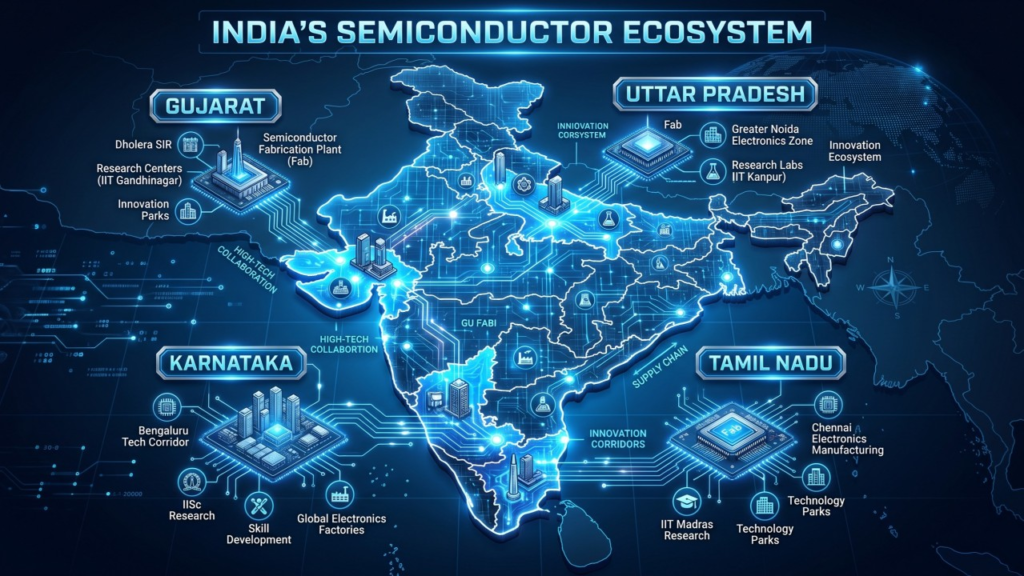
India is undergoing perhaps the most ambitious industrial transformation since the IT revolution. After dominating global chip design for decades, the country is now building a complete semiconductor ecosystem encompassing design, fabrication, packaging, testing, equipment, materials, talent, and infrastructure.
Why Semiconductors Matter for India
Semiconductors are critical to:
- Mobile phones
- Electric vehicles
- Renewable energy systems
- Defence equipment
- Data centres
- AI infrastructure
- Industrial automation
- Consumer electronics
India currently imports the majority of its semiconductor requirements, creating a strategic and economic vulnerability.
The Government’s vision is to transform India from a chip consumer into a trusted semiconductor partner for the world.
Market Opportunity
India’s semiconductor market is expected to grow to approximately US$100–110 billion by 2030, driven by electronics manufacturing, automotive growth, industrial automation, and AI adoption.
India’s Semiconductor Roadmap
Phase 1 (2021–2026): Build the Foundation
India Semiconductor Mission (ISM)
Government support includes:
- ₹76,000 crore (~US$10 billion)
- Up to 50% fiscal support for approved projects
- Design incentives
- Packaging incentives
- Infrastructure support
The objective was to attract anchor investments and establish India’s first semiconductor manufacturing ecosystem.
Phase 2 (2026–2030): Scale Manufacturing
India Semiconductor Mission 2.0
Recent announcements indicate a renewed push through ISM 2.0, with enhanced allocations to deepen domestic capabilities across fabrication, packaging, and supply chains.
Focus areas include:
- Semiconductor fabs
- Compound semiconductors
- Equipment manufacturing
- Electronic components
- Indigenous intellectual property
- Materials ecosystem
Major Semiconductor Projects in India
1. Tata Electronics – Dholera Fab (Gujarat)
India’s First Commercial Semiconductor Fab
Investment: Approximately US$11 billion
Technology Partner: Taiwan’s PSMC
Equipment Partner: ASML
Capacity: Around 50,000 wafers/month
Technology Nodes: 28nm–110nm
Applications:
- Automotive
- AI
- Telecom
- Consumer electronics
Trial production is expected to commence soon.
2. Micron Technology – Sanand (Gujarat)
India’s First Global Memory Packaging Facility
Investment: Around US$2.75 billion
Activities:
- Assembly
- Testing
- Marking
- Packaging (ATMP)
Applications:
- Data centres
- Automotive
- Consumer electronics
This facility places India on the global semiconductor supply chain map.
3. Tata Electronics – OSAT Facilities
Focus Areas:
- Chip assembly
- Testing
- Packaging
Importance:
Packaging is emerging as one of the highest-growth areas globally. India aims to become a major packaging destination.
4. HCL–Foxconn Project
Focus:
- Display driver chips
- Mature-node manufacturing
Potential Applications:
- Smartphones
- Displays
- Consumer electronics
Emerging Semiconductor Clusters
Gujarat
The manufacturing capital.
Hosts:
- Dholera Fab
- Micron
- Tata facilities
- Sanand ecosystem
Karnataka
Strengths:
- Semiconductor design
- R&D
- Start-ups
- Academia
Bengaluru contributes significantly to India’s chip design talent.
Recent initiatives include indigenous GaN testing infrastructure at IISc.
Uttar Pradesh
Emerging Strengths:
- Electronics manufacturing
- Semiconductor assembly opportunities
- Jewar industrial corridor
Tamil Nadu
Advantages:
- Electronics manufacturing ecosystem
- Automotive leadership
- Strong engineering talent base
India’s Competitive Advantages
Talent
India contributes roughly 20% of the world’s semiconductor design engineers.
Global firms operating major Indian design centres include:
- Intel
- AMD
- Qualcomm
- NVIDIA
- Texas Instruments
- Broadcom
- MediaTek
Cost Advantage
Compared to Western economies, India offers:
- Lower engineering costs
- Competitive operating expenses
- Large technical workforce
Strong Domestic Demand
India is among the world’s fastest-growing markets for:
- Smartphones
- EVs
- Consumer electronics
- Industrial automation
Demand itself justifies local manufacturing.
Challenges India Must Address
Talent Gap
India needs thousands of specialists in:
- Process engineering
- Equipment maintenance
- Yield engineering
- Reliability
- Packaging
- Cleanroom operations
Supply Chain Development
Critical gaps remain in:
- Specialty gases
- Chemicals
- Silicon wafers
- Equipment servicing
- Precision components
Infrastructure
Semiconductor fabs require:
- Uninterrupted power
- Ultra-pure water
- Advanced logistics
- Waste treatment systems
Opportunities for Engineering & Project Services Companies
VEN supports activities in:
Pre-Construction
- Design support
- Engineering staffing
- Utility planning
Construction
- Project monitoring
- Quality supervision
- Safety management
- Contractor coordination
Commissioning
- Mechanical completion
- Validation support
- Documentation
Operations
- Facility management
- Maintenance manpower
- Specialist staffing
- Expansion projects
Unlike staffing alone, semiconductor projects demand highly specialised project execution capabilities, where Owner’s Engineering and PMC-type support become valuable differentiators.
Outlook for India
India is unlikely to challenge Taiwan or South Korea in leading-edge nodes immediately. Instead, its realistic strategy is to become:
- A global design powerhouse
- A trusted packaging and testing hub
- A strong player in mature-node manufacturing
- Eventually, a significant semiconductor manufacturing destination
With execution remaining consistent, the semiconductor sector could become for India what IT services became in the 1990s—a transformational industry generating high-value employment, technological capability, and global strategic relevance.